Author: Azya
Posted: 2025-11-06 08:22
Original: Article link
I continue the series of articles (part one, part two) about “Tetris” games and the microcontrollers used in them. In the previous parts, we described the 4-bit Holtek controller, variations of which were used in Brick Game and many other portable electronic games released in the 1990s.
Since then, I have decapsulated (the process of extracting the chip from the IC package) and photographed under a microscope more than a dozen chips from this family across various games. Among them were familiar Brick Game units and different electronic keychains, as well as games from well-known manufacturers, like Nintendo Mini Classics and Bandai Mame series. For nine of these, I was able to read the ROM and add it to the emulator from the previous article.
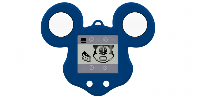
A virtual pet that also runs on 4-bit Holtek
Naturally, I encountered microcontrollers not only from Holtek but from other manufacturers as well. I studied them too and, where possible, dumped and emulated them. One such chip will be described in more detail in this article.
Apollo 126 in 1 English Talking (B0202)
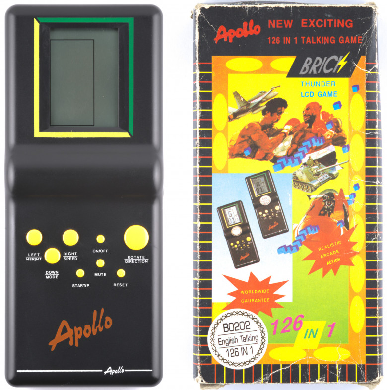
Typical Apollo case and box
My unit was released in April 1995. The case is black, standard for the Apollo line. The segment layout on the display is exactly the same as many other Brick Games, including the E-23 from the previous article. However, the game selection is slightly non-standard: in addition to regular Tetris and various racing-shooting games, there is a Frogger-like game and a slot machine. Another distinguishing feature is the voice commentary accompanying the games.
Under the drop of compound, I found a Sunplus microcontroller labeled PA2071-160:
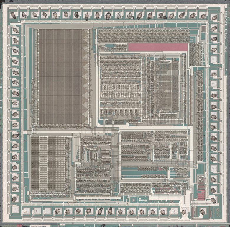
Sunplus chip with PA2071-160 marking on the die
The first task was to determine the chip’s model or at least its family so that we could try to find documentation. We can gather several parameters from the photo: manufacturer Sunplus, 20 KB ROM, 192 B RAM, LCD driver with 40 segments and 8 common lines, 8-bit 6502 core. Additionally, since the game had voice commentary, the controller should have that capability. With this information, I went to archive.org and looked at the earliest Sunplus backups, finding tables like this one to match it as closely as possible to SPL02B. Note the slight ROM size mismatch: listed as 19.5 KB, ours appears as 20 KB; the reason will become clear later.
Documentation for SPL02B is fortunately available, though very superficial, which is typical for specialized microcontrollers of that era.
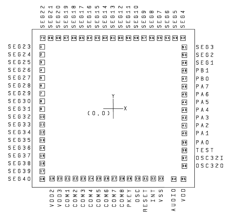
There is also a minor discrepancy in the pads: our chip has two extra pads around VDD2 and VDD3 that are not on the datasheet diagram (left image). It’s unclear why: either the microcontroller is not exactly SPL02B but perhaps SPL02A (for which documentation was not found), or the pads were never intended for probing, suggested by the absence of test marks.
Despite these minor mismatches, the microcontroller is identified, and its specs can be assessed from the official documentation: 8-bit core (a reduced 6502 variant) with a frequency up to 1.5 MHz, 19.5 KB ROM, 192 B RAM, support for a 32 kHz crystal, and the sound system includes two tone channels, a noise channel, and a voice channel. Clearly, the specs are significantly higher than the Holtek chips described in the previous article.
Let’s examine each parameter in more detail.
6502 Core
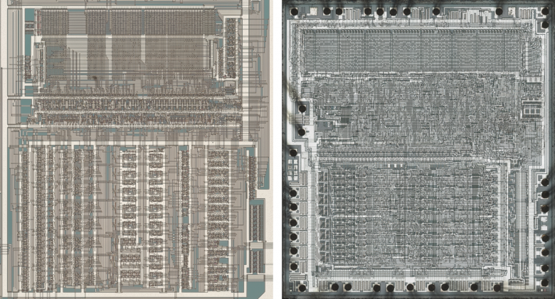
Comparison of SPL02 and 6502 cores (original photo)
In the photo, the SPL02 core is on the left and the original MOS 6502D is on the right. The topologies are completely different, but the structure remains: instruction decoder on top, 8-bit ALU below, and control logic in between.
ROM
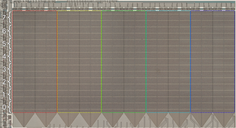
ROM on the die
The numbers on the left indicate areas corresponding to the bits of each digit, and colored rectangles mark regions of the main program memory and four additional banks. If you flip the address space map from the datasheet, the order of the ROM blocks will match what we see in the photo:
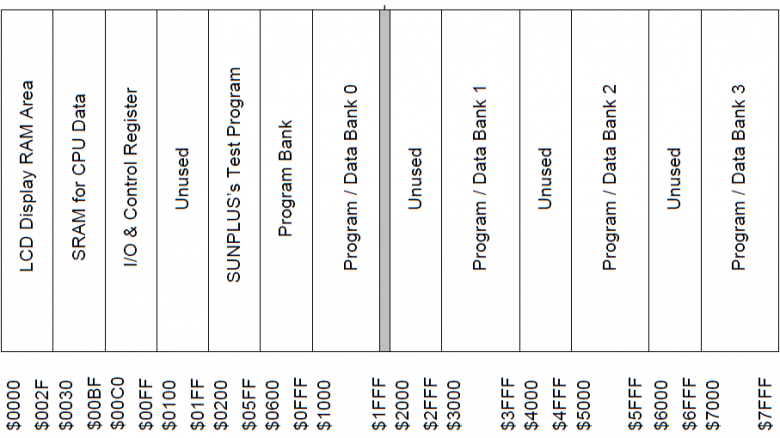
By studying the ROM structure, we can understand the reason for the discrepancy between the actual memory size and the documentation: the first 512 bytes, allocated for RAM and registers, are physically present on the chip but not addressable. If you zoom in on the section of ROM containing every zero bit, which occupies addresses $0000–$07FF, you can see that the first 512 bytes are simply filled with zeros (the same pattern is observed for the other bit planes):

ROM section containing every 0th bit from 2048 bytes of main memory
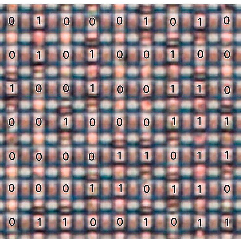
Fragment of ROM with labeled cell states
On the left is a zoomed-in fragment, outlined in red, where the memory cell values are labeled. It is clear that the resolution of the image leaves something to be desired, but I simply do not have sufficiently high-quality lenses to photograph large areas of such a dense process. Even so, the bits are readable, and by adjusting focus and aperture, I was able to produce photos suitable for automatic recognition using contrast differences, with an acceptable number of errors, in the thousandths of a percent. But even thousandths of a percent of 163,840 bits are hundreds of errors scattered across an image with a resolution of about 6500×14,000 pixels, which I then found and corrected manually, bit by bit. A long and tedious job.
Photos of the entire ROM in two shooting variants can be found here.
RAM
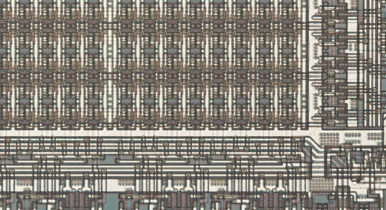
RAM fragment with control logic
The RAM size is 192 bytes: the first 48 bytes are video memory, where every 6 bytes are allocated per common line, and each bit in this block controls one of 48 segments. Since the microcontroller only supports 40 segments, every sixth byte is unused. The remaining 144 bytes are available for general-purpose use and for stack organization.
Input/output and control registers
As with most microcontrollers, the SPL02 has special registers that control peripherals and operating modes. 64 bytes are allocated for these at addresses $00C0–$00FF, although only 14 registers are actually used. This is one of the main challenges when emulating this microcontroller, because the datasheet describes the registers only in general terms, and for most of them, addresses are not even specified. Part of this problem was resolved with the G+ IDE for 6502, which includes header files for this microcontroller with a more detailed description of the registers:
;----------------------------------------------
;      I/O configuration for hardware system
;----------------------------------------------
  P_C0H_IO_Ctrl                  EQU     0C0H
  ;??       duty
  ;  ?      cpu clock
  ;   ?     Frosc
  ;     ?   port b 1:0
  ;      ?  port a 7:4
  ;       ? port a 3:0
  P_C1H_PortA_DataPort           EQU     0C1H
  P_C3H_PortB_DataPort           EQU     0C3H
  P_C4H_Freq_ToneA               EQU     0C4H
  P_C6H_Freq_Vol_ToneA           EQU     0C6H
  P_C8H_Freq_ToneB               EQU     0C8H
  P_CAH_Freq_Vol_ToneB           EQU     0CAH
  P_CCH_Noise_Type               EQU     0CCH
  P_CEH_Noise_Vol                EQU     0CEH
  P_D0H_Standby_Normal_Config    EQU     0D0h
  P_D2H_INT_Config               EQU     0D2h
  P_D4H_Speech_Mode              EQU     0D4h
  P_D5H_Speech_Data_Port         EQU     0D5h
  P_D7H_Bank_Select_Port	     EQU	 0D7h
Sound
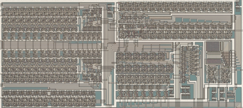
Main logic of the sound generator
A distinctive feature of this microcontroller is the presence of a 7-bit DAC through which sound is output from two tone channels, one noise channel, and a speech channel, which directly controls the DAC via the Speech register. Thanks to this, it is possible to play 7-bit sound programmatically – this is exactly what allows the Apollo Tetris to comment on the game with various short, unintelligible phrases.
In fact, even with just seven bits, reasonably good sound can be produced at a high enough sampling rate, but due to the limited ROM size, the developers could not fully exploit the microcontroller’s potential. I studied the playback code a bit and discovered that the phrases are stored in 4-bit PCM, two samples per byte, which are then mapped via a lookup table to the full 7-bit range and played back at around 6 kHz. Even with such limitations, half a second of playing the word “Apollo” occupies 1,406 bytes.
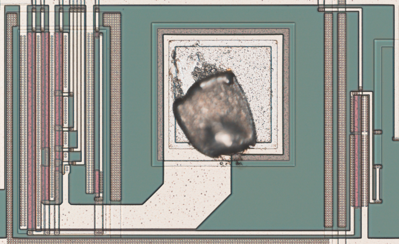
Here you can see how 7 digital lines coming from the top-left control the current on the audio output in the center
Emulation
I ended the previous article mentioning the BrickEmuPy emulator, which I initially wrote for Holtek microcontrollers, specifically for the E-23. At first, I thought I would stop there, but the topic of emulation fascinated me so much that I started buying other “Tetris” games and, in general, all games with segmented LCD screens from the 1980s–1990s, decapsulating them to obtain firmware and adding them to my emulator.Naturally, not all purchased games used Holtek microcontrollers, but if the microcontroller had ROM that I could read optically, I added them to BrickEmuPy as well. The SPL02 became the 11th family of microcontrollers supported by BrickEmuPy, and the total number of games now approaches 50.
Video demonstrating emulation of Apollo 126 in 1:
Running external code
While debugging the B0202 emulator on the obtained ROM image, I came across an interesting section of code invoked by an external interrupt:
2FC0:	sei            ;78
2FC1:	lda #$CB       ;A9CB
2FC3:	sta $C0        ;85C0
2FC5:	lda #$00       ;A900
2FC7:	sta $C6        ;85C6
2FC9:	sta $CA        ;85CA
2FCB:	sta $CE        ;85CE
2FCD:	lda #$01       ;A901
2FCF:	sta $C3        ;85C3
2FD1:	lda #$00       ;A900
2FD3:	sta $C3        ;85C3
2FD5:	ldx #$00       ;A200
2FD7:	lda $C1        ;A5C1
2FD9:	sta $38, X     ;9538
2FDB:	lda #$02       ;A902
2FDD:	sta $C3        ;85C3
2FDF:	inx            ;E8
2FE0:	lda #$00       ;A900
2FE2:	sta $C3        ;85C3
2FE4:	cpx #$78       ;E078
2FE6:	bne 2FD7       ;D0EF
2FE8:	lda #$01       ;A901
2FEA:	sta $C3        ;85C3
2FEC:	jmp 0038       ;4C3800
;when will Habr finally start supporting different assembler notations :(
This is a debug mode that allows executing external code even after the chips with mask ROM have been manufactured at the factory.
To put it mildly, I was intrigued by the possibility of running my own code on "Tetris." My first thought was to buy the same B0202 and try to invoke this debug mode, but I already had another Apollo – 18 in 1 B0302 – waiting for its turn. Its pinout turned out to be very similar to the B0202, so I assumed it used the same or a similar microcontroller and started experimenting on it.
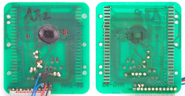
B0302 main board. The pins used in debug mode are marked in red.
The first problem, which could have been the only and insurmountable one, was that the external interrupt is not routed on the chip, so it cannot be triggered normally. However, it turned out that by inducing noise on the clock-setting resistor, the microcontroller is very likely to jump to the external interrupt vector. That is, simply touching the clock-setting resistor on the board with a finger showed me on the pads connected to the 2 least significant bits of port B the cherished picture of transfer clocking, with timings corresponding to the code above. Later I noticed that even simply reinserting the battery sometimes produced the same result (many probably remember strange bugs appearing when changing batteries as kids).
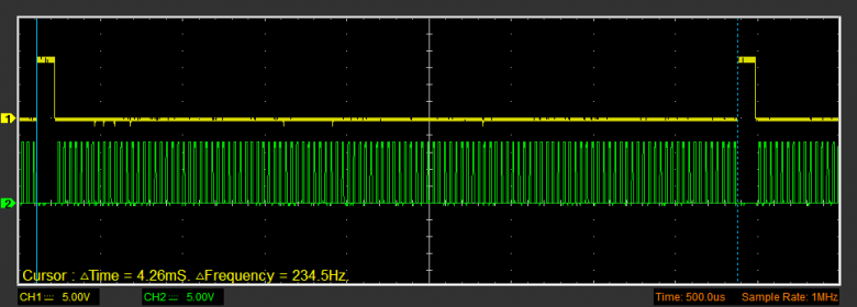
Channel 1: port B line 0; Channel 2: port B line 1.
First, I tried sending instructions simply by pressing the buttons on the "Tetris." Of course, this would be one instruction repeated 120 times, but it was enough to test the theory. And yes – it worked: the microcontroller predictably paused the transfer for the number of clock cycles corresponding to the number of instructions sent. At this stage, I faced the second difficulty: only the 7 least significant bits of port A are connected to the buttons, so any instructions using the high bit could not be transmitted directly. How I worked around this will be explained shortly.
The next task was to create a data source that would, based on the clock signal from port B,
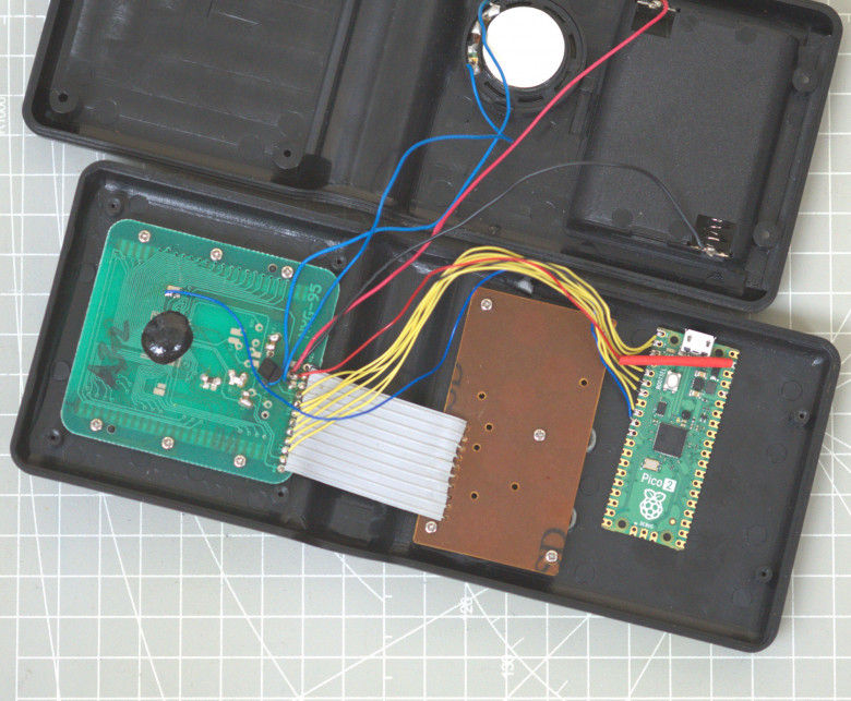
Everything was ready to transmit a meaningful set of instructions, but first, the missing high-bit problem needed to be solved. Initially, of course, I tried simply not using such instructions. Here I encountered another problem: programs ran incorrectly when instructions with absolute addressing were used. It turned out that, unlike the B0202, the debug mode of the B0302 stores received data starting not from $0038, but from $0000. Once I figured this out, I was finally able to run my code. I don’t remember exactly which code, but, for example, it could have looked like this:
0000: sec

loop:

0001: rol $00

0003: jmp loop
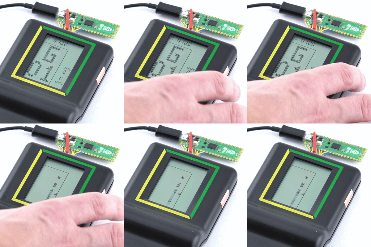
The execution result is shown in the GIF on the left. The program simply shifts the zero byte in RAM endlessly, and the segments addressed to it start flickering. The static segments are pieces of the program itself, since it is located in the RAM area allocated for video memory. Notice the method of execution: I attached copper tape at one end to the traces near the chip and at the other end to the Apollo case, so there was no need to open it to trigger the interrupt.
Of course, having only half the instructions limits what you can write. You need to add some corrective code before executing the main block of the program, and the best idea I came up with was to transmit each byte using the high bit shifted right, and in the corrective part, shift it back through the carry flag, first setting or clearing it according to the least significant bit. My perhaps confusing explanation is better illustrated with code:
;corrective code

0000: sec

0001: rol $03

;code to be corrected

0003: .byte $54, $00

;after executing the first two instructions, "54 00" will become "A9 00"

;which corresponds to the previously inaccessible instruction lda #0
dataSize = 74
;correcting the main code using the method described above
sec
rol $17
rol $0E
rol $10
rol $15
sec
rol $16
rol $1B
;main code correcting the data
ldx #dataSize-1

mainLoop:
inc loBitPtr+1
clc
loop8:
loBitPtr:
ror loBit1
beq mainLoop
lda data, X
rol
pha
dex
bmi start
jmp loop8
loBit:
;here lie the least significant bits

* = 120-dataSize

data:
;here are the bytes shifted right

* = 128-dataSize

start:
In Python, I wrote a script that accepts up to 74 bytes of machine code, merges it with the program above, and sends the complete 120 bytes to the Pico. The entire process is now automated: all that’s left is to touch the clock-setting resistor on the Apollo, and the Pico will transmit the program, which immediately begins execution.
Reading the firmware
The first step was to write a program that transmits the B0302 firmware via port B:
ldx	#$00
lda #$00

bankLoop: ;iterate over ROM banks
sta $D7 ;store the current bank number in the bank select register D7
byteLoop:
lda (romPtr, X) ;fetch the next byte from ROM
rol
ldx #$08
bitLoop: ;shift this byte bit by bit
and #$FE
sta $C3 ;and send it via the 1st bit of port B
ora #$01
sta $C3 ;and clock the transfer via the 0th bit
ror
dex
bne bitLoop

inc romPtrL        ;increment the 16-bit address
bne byteLoop
inc romPtrH
lda romPtrH
cmp #$20
bne byteLoop       ;until the end of the bank is reached
lda #$10           ;all banks start at $1000
sta romPtrH

inc bank           ;move to the next bank
lda bank
cmp #$04
bne bankLoop       ;until the last possible bank is reached
brk                ;after completing the transfer, start over

romPtr:
romPtrL:
.byte $00
romPtrH:
.byte $00
bank:
.byte $00
It turned out that the B0302 has only two ROM banks (data is repeated in the others), i.e., a total of 11.5 KB of ROM. If we refer to the same table of microcontroller specifications, such a size exists only in the SPL03. This means that the two Apollo boards contain slightly different controllers, and it can be assumed that the numbers in the B0202 and B0302 game codes indicate their index. It also becomes clear why the data is stored starting at $0000 instead of $0038 – the RAM here is even smaller than in the B0202, only 128 bytes. Another unfortunate limitation: instead of a 7-bit DAC, the SPL03 has only a 6-bit PWM, and it’s split across two pins, whereas the Apollo design uses only one, meaning effectively only 5 bits can be used for audio output.
Bad Apollo
Initially, I planned to write a simple game, but once it became clear that the total available memory is not 192 bytes but only 128, I had to abandon that idea. I then decided to write a player for "Bad Apple!!" – a visually striking demo for running on the "Tetris," which, if transmitted uncompressed, is relatively simple to implement.Video and audio are stored on the Pico 2, which acts as external serial-access ROM, while the program on the Apollo requests and receives data synchronized to the frame rate, which is 1/16384 of the microcontroller’s clock frequency, roughly 42 frames per second. Most of the data is audio in the form of 5-bit PCM at approximately 22 kHz.
After some experimentation, I settled on the following data format:
Each transmitted byte (without the high bit, as you recall) contains a 5-bit audio sample and 1 bit for the state of a single segment. I allocated 32 SPL03 core cycles to process one byte. During this time, the byte must be requested, received, the sample loaded into the voice port, and the corresponding segment turned on or off. Total video memory on the SPL03 uses 32 bytes, but they are spread over 48 bytes, which I rounded up to 64 for convenience. Thus, each frame takes 64 × 8 × 32 (*) = 16,378 cycles, meaning the display updates in sync with the LCD frame rate – exactly what was needed. The audio sample rate becomes 1/32 of the microcontroller frequency, which for the B0302 is roughly 21.7 kHz – more than sufficient; higher-quality uncompressed audio simply won’t fit in the 4 MB of Pico 2 flash.
(*):
64: Size of video memory rounded to 64
8: Bits per byte in video memory
32: Core cycles to process one received byte
Data Preparation
There were no issues with the audio: I simply opened the original video track in Audacity and exported it as 8-bit raw PCM at the required sample rate.Video required more work. First, I had to decide on the frame rate – the original video is 30 FPS, while the B0302, as mentioned, runs at 42 FPS. There are two options: duplicate some frames to adjust the original frequency to 42 FPS, or drop frames down to 21 FPS (half the needed frequency) and use the extra frames to simulate additional grayscale levels. After comparing both approaches, I chose the second.
Audio and video are combined by a Python script, which discards the 3 least significant bits of the audio stream, placing the remaining bits in positions 5–1 (6–2 positions: this minimizes processing on the Apollo, as the SPL03 expects data in this format in the Speech port). The least significant bit sets the state of one of the 256 segments sequentially, frame by frame.
Player
The data is prepared; now it’s time for the code that will play it back on the Apollo:
* = $36

ldx #$36
txs
jsr clearLCD

lda #$01
sta $D4            ;enable Speech Play Mode

main:
ldx #00
mainLoop:
lda #$02 ;request the next byte from Pico
sta $C3 ;on the rising edge of B1
lda #$00
sta $C3
lda $C1 ;receive it from port A
sta $D5 ;and immediately write it to the Speech port

ror 		       ;save the 0th bit with the segment state into the carry flag
lda segStates
rol                ;shift segStates left, adding the new segment state
bcc byteNotFull    ;and simultaneously check if a full byte has been received
sta $00, X         ;store the received byte in video memory
inx

lda #$02	       ;then duplicate the same process as above, but
sta $C3            ;with slight modifications to avoid delays
lda #$01	       ;related to storing the byte in video memory
sta $C3            ;to fit exactly into 32 cycles
sta segStates
lda $C1
sta $D5

ror
rol segStates

cpx #64            ;iterate over all 48 + 16 bytes of video memory
beq main           ;safely overlapping code area
jmp mainLoop

byteNotFull:
sta segStates
jmp mainLoop

segStates:
.byte 01

* = $055B

clearLCD:
Here’s what the result looks like:
Conclusion
Of course, Bad Apollo is just a demo to attract attention. The main and most difficult part of this work was obtaining the firmware for two other Brick Game models from the ’90s, which allowed writing emulators and preserving them for history (as pompous as that may sound).I hope that over time it will be possible to dump other Apollo models, which apparently numbered at least a dozen. But, of course, it is not guaranteed that it will be as easy to trigger an external interrupt on all of them – for example, I tried the same thing on the Apollo 12 in 1 and nothing worked.
If anyone reading this article wants to experiment with other Apollo models, please share your results in the comments or contact me directly, even if the results are negative. I will do my best to answer any questions.
The source code described in this article is published on GitHub
Photos and other materials on the Apollo B0202 are published on archive.org
>> Home